
Featuring a straightforward design, the 15-watt stereo amplifier circuit excels in delivering impressive dynamics and outstanding bass reproduction. Despite its modest power output of 2x15W RMS, it proves ideal for use in smaller spaces like apartments. Pairing it with speakers boasting a minimum power rating of 20W ensures a thoroughly satisfying audio experience.
Block Diagram
The amplifier's functional diagram, depicted in Figure 1, is straightforward and does not necessitate any particular comments.

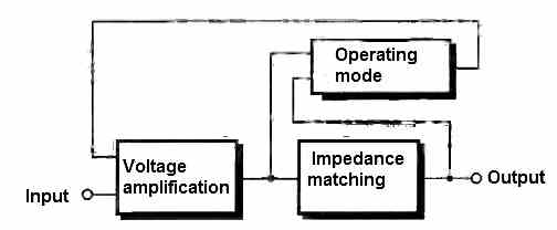
One can readily discern the ability to choose between operating modes, allowing the amplifier to operate either in pure class AB or in feedback-controlled class AB.
The feedback-controlled mode provides the benefit of increasing output power without the need to worry about thermal runaway in the power transistors. Conversely, the absence of feedback enhances the dynamic response of the amplifier.
Circuit Description

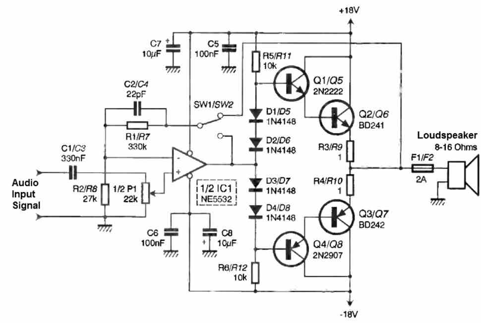
Understanding the functionality of this 15-watt stereo amplifier circuit involves the following key points:
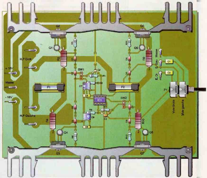
- Voltage amplification is achieved through operational amplifier IC1, configured as a non-inverting amplifier with a gain of 1 + R1/R2 = 13.2.
- Capacitor C1, in conjunction with potentiometer P1, creates a low-pass filter with a cutoff frequency (F1) of 1/(2πC1P1) = 10.9 Hz.
- A high-pass filter is formed by C2 and R1, resulting in a cutoff frequency (F2) of 1/(2πC2R1) = 21.9 kHz.
- The amplifier can operate in either feedback-controlled class AB or non-class AB, determined by jumpers SW1 and SW2. Connecting R1/C2 to R3/R4 enables global feedback; otherwise, feedback is local.
- Global feedback allows for additional power but requires replacing resistors R3 and R4 (1 Ω 3 W) with 0.1 Ω 1W resistors.
- Resistors R5 and R6, along with diodes D1 to D4, maintain slight conduction in the output transistors, ensuring class AB operation.
- Reducing the values of R5 and R6 increases transistor bias current, moving away from class B operation and preventing crossover distortion.
- Capacitors C5 to C8 are responsible for filtering the power supply voltage.
Now, let's delve into the power supply voltage filtering aspect.
Power supply Circuit
A transformer equipped with dual secondary windings supplies us with 18 volts, which will subsequently undergo rectification via diode bridge P1.

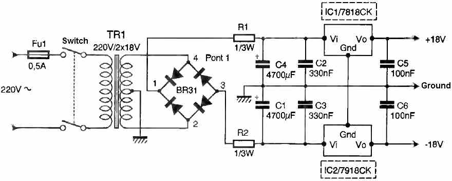


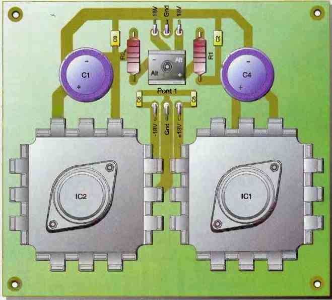
This circuit generates two stabilized DC voltages, +24V and -24V, utilizing capacitors C1 and C4 for voltage regulation. C1 and C4 function as energy storage components, while C2 and C3 act as filters to eliminate unwanted noise.
Resistors R1 and R2 play a crucial role in limiting the current during the initial charging of the capacitors, ensuring a controlled voltage drop. Following this, IC1 and IC2 are employed to regulate and maintain the voltages at +18V and -18V.
How to Build
Implementing the two input circuits is straightforward, regardless of whether a photographic method is employed or not.


Caution is advised when working with the power circuit, and it's essential to avoid narrowing the width of the large traces, given the substantial currents, which can reach several amperes.
Initiate the assembly process by soldering the smaller components such as jumpers, diodes, and resistors. Follow this with the integration of the circuit and small SMD capacitors.
Conclude the assembly by incorporating the transistors, fuse holders, power resistors, and the potentiometer. When selecting heat sinks for the power transistors, opt for models with a maximum value of 2°C/W.
Ensuring a secure attachment of the heat sinks to the printed circuit board is crucial to prevent potential damage to the transistor leads caused by handling and vibrations.
Finally, remember to insulate the power transistors from the heat sink using silicone insulators and insulating washers to maintain proper functionality.
How to Test
Caution is advised when working with the power circuit, as the currents can reach several amperes. It's crucial not to restrict the width of the large traces during assembly.
Commence the soldering process by attaching small components such as jumpers, diodes, and resistors. Proceed to install the integrated circuit and small SMD capacitors. Conclude the assembly with the placement of transistors, fuse holders, power resistors, and the potentiometer.
For the power transistors, opt for heat sinks with a maximum value of 2°C/W. Ensure a secure attachment of the heat sinks to the printed circuit board to prevent damage from handling and vibrations.
Remember to insulate the power transistors from the heat sink by utilizing silicone insulators and insulating washers. This precautionary step is essential to safeguard against potential issues.