
A 24 V DC supply may be efficiently converted into a 12 V DC output using the buck converter circuit that is presented below. In other words, the circuit will let obtaining a 12 V DC with very little power loss from a 24 V DC source.
Compared to linear regulators like IC 7812, IC LM317, or IC LM338, this buck converter circuit is extremely efficient and won't lose or waste electricity.
Why Buck Converter is Better than Linear Regulators
Because of the way they operate, linear regulators like the LM317 and 7812 are regarded as poor step-down converters.
Heat is produced during the dissipation of surplus input voltage in a linear regulator. According to this, the voltage difference that exists between the input and the output ends is merely "exhausted" off" as power that is not used. Just like a variable resistor, the linear regulator dissipates extra power and controls the output voltage by varying its resistance.
This dissipating mechanism causes major energy waste along with poor efficiency. The ratio of output power to input power establishes a linear regulator's efficiency. Heat is the result of the voltage difference multiplied by the output current, and it grows with the input-output voltage differential. As a result, efficiency decreases as the input and output voltage difference increases.
An example of this would be the dissipation of heat caused by a linear regulator regulating a 24 V input down to 12 V. In situations requiring high power, this can lead to significant power waste and need extra cooling methods.
Comparatively, step-down conversion is more effectively accomplished by switching regulators, including buck converters. To effectively convert the voltage, they use an arrangement of switches, capacitors, and inductors.
In order to reduce the amount of energy lost as heat, switching regulators conserve power throughout one part of the process of switching and distribute it through other. Switched regulators are capable of reaching efficiency of 80–95% and possibly greater according to the particular configuration.
In conclusion, even though linear regulators like the LM317 and 7812 are simple and affordable, these are not the best option for step-down conversion unless power efficiency is a major consideration.
Understanding the Circuit
The fundamental schematic of the 24 V to 12 V converter is seen in the image below.

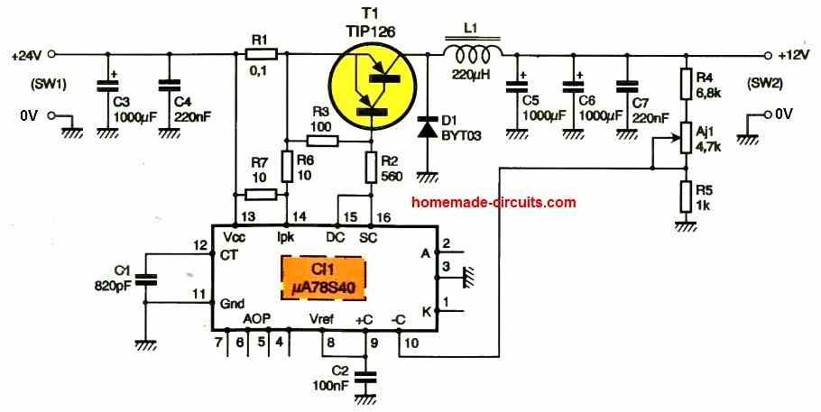
The Motorola µA78S40 is a widely used buck converter regulator device.
The on-chip layout of this integrated circuit, that has the oscillator, flip-flop, comparator, voltage reference source, driver, and switching transistors required for a switching regulator, is shown in the accompanying figure.

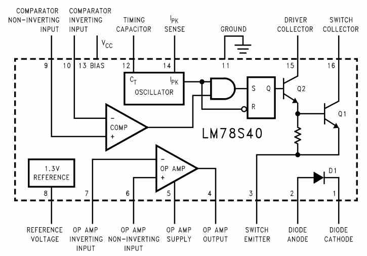
An operational amplifier is also present, although it is not required for the present application. Capacitors C3 through C7 execute the power supply's filtering and smoothing.
The frequency of the oscillator is set by capacitor C1, and resistors R1, R5, and R6 assist in limiting the converter's output current.
The converter's output current determines the voltage over resistor R1.
Resistors R6 and R7 establish a voltage divider by establishing a voltage differential of approximately 0.3 V between pins 13 and 14 of the µA78S40. This allows current limiting to start at roughly 5A.
Pin 8 of IC1 provides access to the voltage reference source, which is separated by capacitor C2.
The non-inverting input of IC1's internal comparator receives this reference voltage. A voltage level proportionate to the output voltage of the converter is established for the inverting input.
The comparator regulates IC1's output stage in order to keep the output voltage steady.
The expression below provides the output voltage of the comparator, which has both of its inputs kept at an identical voltage:
Vs = 1.25 * [1 + (R4 + Aj1) / R5].
The adjustable resistor Aj1 allows for adjusting the converter's output voltage in the range of +10V to +15V.
The two output transistors form a Darlington pair, and their successive switching is controlled by the flip-flop in sync with the oscillations of capacitor C1.
Combined with an AND gate, this flip-flop is controlled by the comparator to adjust the conduction time of the output stage of the µA78S40 and maintain a constant output voltage.
Transistor T1's saturated or inhibited condition corresponds to the Darlington pair condition of IC1. Transistor T1 is biased and resistor R2 limits its base current when IC1's output stage is saturated.
In order to limit the VBE voltage of transistor T1 at the start of the switching operation, resistor R3 and resistor R9 create a voltage divider.
At the oscillator frequency of the µA78S40, transistor T1, functioning as a Darlington model, exhibits the characteristics of an open or closed switch.
The characteristics of inductance enable the voltage drop between 24V to 12V in the inductor L1. In the constant situation, inductor L1 is subjected to a voltage of +12V while transistor T1 is saturated.
The coil accumulates energy throughout this phase, which it discharges once the applied voltage is removed. Therefore, inductor L1 prefers to keep the electrical current traveling via transistor T1 regardless of whether it is blocked.
A reverse EMF spike of -12V occurs across inductor L1 as diode D1 turns conductive.
This back EMF, which exists across capacitors C5 and C6, is caused by the conduction of diode D1, which guarantees the continuing existence of their charge.
Transistor T1 resumes conduction whenever the charge level in IC1 falls beneath the comparator's cut-off limit.
Voltage sinks brought on by the forward voltage of diode D1 and the saturation voltage of transistor T1 are not taken into consideration in this concise description of this 24V to 12V buck converter functioning.
The capacitance is one of the components that affects the converter's residual output ripple.
How to Build
The arrangement of the PCB tracks that will be replicated using the technique of your choosing is depicted in the figure below. Broad dimensions main power lines are needed to handle heavy currents.

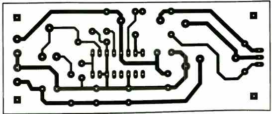
These rails could be tinned to improve their conductivity soon after the circuit has been printed and etched.
The component positioning is displayed in the following Figure.

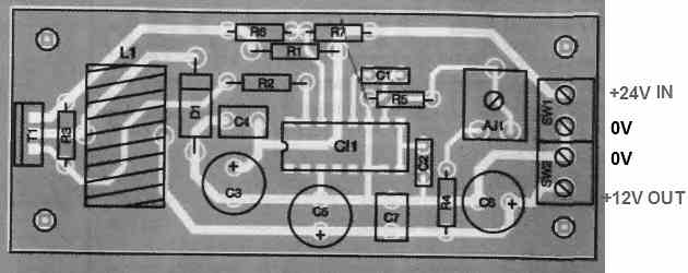
Enameled wire with a 1 mm thickness may be wound onto a high-flux toroid having an outside diameter of 21 mm and an inner diameter of 12.5 mm to create the inductor, which is a 5A toroidal type.
Because a toroidal inductor offers a higher saturation flux density (two times more), it is advised that you employ one instead of a choke coil, such as ones that are utilized for triac noise reduction.
A couple of 0.22 Ohm / 1W resistors wired in parallel could be used to substitute of the tiny 0.1 Ohm current-limiting resistor R1.
Because capacitor C3 has an alternator/regulator system that keeps the battery charged, it could encounter voltages higher than 24 volts when the car is operational.
Consequently, this capacitor has to have an operating voltage of no less than 35V. To guarantee that the heat sink's temperature stays within an appropriate range when operating continuously, it must be chosen with a thermal resistance of no more than 3°C/W.
A mica insulator and an insulating sleeve should be used to isolate the switching transistor T1 from the heat sink.
Enhancing heat dissipation is possible with silicone grease application. Clean the mica insulator on both sides with a thin coating of silicone.
Automobile lamps with a voltage of 12 V may be employed as a load for testing, and the output voltage can be changed with the help of the adjustable resistor Aj1. The whole thing is supposed to be placed within a metal enclosure.