
Class B and AB power amps are very popular among HI-Fi enthusiasts, because they can deliver high-quality sound with low distortion and high efficiency. But how do they achieve this? What is the difference between class B and AB?
In this model, you can discover the principles behind these power amps and experiment with different configurations. You can change the bias voltage, the input signal, the load resistance, and the feedback network. You can also compare the output waveforms and measure the power dissipation and efficiency. This is a great way to learn more about these fascinating power amps.
Understanding Power Amplification Classes
The operating class of a power amplifier depends on how long the power transistor conducts during each cycle of the input signal. This is how power amplifiers are classified.
Class A Amplifiers
In a class A amplifier, the output stage has one transistor that conducts for the entire duration of each signal cycle.
Class B and Class AB Amplifiers
In class B amplifiers, one transistor conducts for half a cycle and another for the other half. Class AB amplifiers are similar but more popular. The difference is in how they are biased to reduce the effects of the base-emitter junction threshold, which can cause distortion when the transistors switch on and off.
Characteristics Illustrated
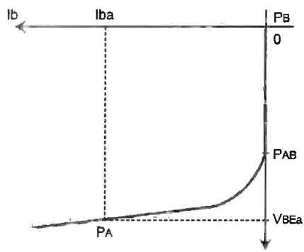
The characteristic curve Ic = f(Vbe) of a silicon NPN transistor shows the operating points PA, PB, and PAB in Figure 1. These points represent the amplification classes A, B, and AB, respectively.

PNP Transistor Configuration
A PNP transistor has opposite polarities for Ic and Vbe. Figure 2 shows a basic diagram of a single-transistor amplifier that works in class A, with base biasing provided by the resistors Ra and Rb.

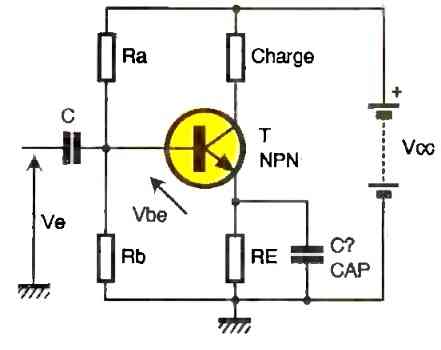
To ensure that the voltage Vbeo is equal to Vbea (value shown in Figure 1) when there is no excitation (ve=0), these two components must be calculated accordingly.
A class A amplifier has significant drawbacks, such as high power consumption even at rest and a maximum efficiency of only 25%.
Class B and AB amplifiers are more preferable, as they offer much higher efficiency (up to 78% maximum) and negligible or zero power consumption at rest.
The following diagram illustrates the basic design of a class B amplifier without any additional features.

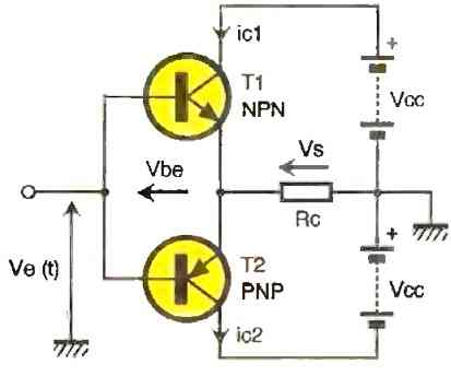
The input signal ve(t) connects to the bases of the two complementary transistors, T1 and T2, which are also interconnected.
There is no biasing at the base level, so the voltage Vbeo is zero when the control signal (ve(t)) is absent (ve(t) = 0).
The emitter current iel is proportional to the collector current ic1 (= β1 * ib1) when the input voltage ve(t) exceeds the conduction threshold of the NPN transistor T1, causing it to turn on. The load current flows through T1 during the positive half-cycle of ve(t).
The PNP transistor T2 is off when T1 is on, and vice versa. The load current flows through T2 during the negative half-cycle of ve(t), when the input voltage ve(t) falls below the conduction threshold of T2, causing it to turn on.
The input voltage ve(t) shows up again across the load because of the voltage drop over the base-emitter junctions.
A class B stage has a voltage amplification that is a bit lower than 1, but it can boost the current a lot since the input and output currents match the base and emitter currents of the transistors.
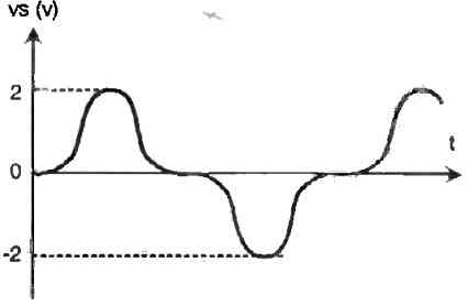
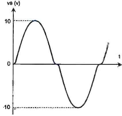
When the input voltage ve(t) is low (a few volts), the output signal is distorted because of the transistors' conduction threshold. This distortion becomes less noticeable as ve(t) gets higher (See Figures 4a and 4b below).


The previous circuit is modified as shown in Figure 5 below to reduce this distortion. The bases of the two transistors have a slight bias.

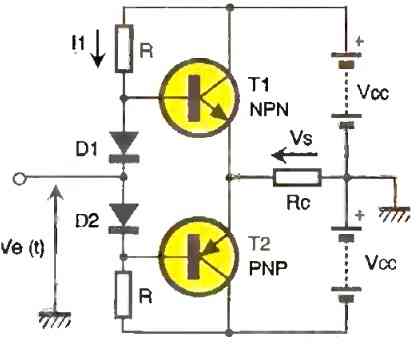
A class AB amplifier is used. Diodes D1 and D2 have a current flow 11 that causes a voltage drop across them. This voltage drop biases transistors T1 and T2 at the PAB point, as shown in Figure 1.
By pre-biasing, the base-emitter junctions of T1 and T2 are made ready to conduct without a conduction threshold. The output signal vs is similar to ve(t).
The term "pre-biasing" is better than "biasing" because it implies that the transistor is barely conducting or not conducting at all, but it can start conducting when needed.
To reduce the distortion rate of power amplifiers, only a few components are needed to switch from class B to class AB.
Hence, it is clear that this structure is widely used by most power amplifiers. Although it may not always appear in the exact form proposed, its different variations always have the same function.
Prototype Specifications
A symmetrical power supply of ±15V relative to ground, with a 1A current capacity, powers the prototype. The load is a 10 Ohm resistor that can handle at least 5W of power.
This value, though small, is important because it helps us deal with some problems related to the heat generated by the load or power transistors, which have heat sinks attached to them.
To switch from class B to class AB, we need to move some tiny jumpers that are like the ones used in computers.
A possible way to examine the effects of global feedback on the load is to combine the power amplifier with an operational amplifier. This feedback loop connects the load to the output of the operational amplifier.
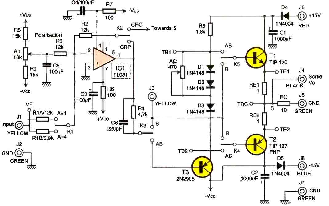
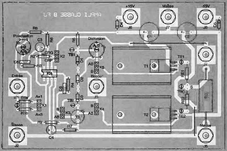
Schematic for the Amplifier Prototype
The first part of this article mentioned some sub-assemblies, such as transistors T1 and T2. Figure 6 shows these sub-assemblies.

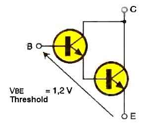
A Darlington transistor is a type of transistor that has a very high current gain β, usually over 1000, compared to ordinary power transistors that typically have β values around 100. This means that the base current lb of a Darlington transistor can be much smaller than that of a regular transistor. Figure 7 below shows the schematic of a Darlington transistor.

A possible drawback of this option is that it raises the conduction threshold of the transistors (twice 0.6V), which helps to better assess the shortcomings of a class B amplifier at low levels, but also needs to be considered when choosing the biasing system for switching to class AB.
Aiming to stabilize the output stage against temperature changes, we added two emitter resistors (RE1 and RE2) that were not in the theoretical diagrams of Figures 3 and 5.
When the temperature rises and the base current stays the same, the emitter current lel also rises from its value at temperature θ1.
This makes the transistor dissipate more power, which makes the temperature go up even more. This vicious cycle can destroy the transistor very fast if it is not controlled properly.
The resistor RE stabilizes the emitter current by creating a negative feedback loop. When the emitter current increases, the idle voltage Vbeo drops, which reduces the base current lb and the emitter current. This also lowers the power dissipation and the temperature of the transistor, counteracting the initial increase in temperature.
Because the transistors T1 and T2 are Darlington pairs, they have a conduction threshold that is twice as high as a normal transistor. Therefore, the biasing circuit for these transistors requires 3 diodes.
Ideally, 4 diodes should connect the bases of T1 and T2.
A better way to write the text is: To pre-bias the two transistors at about 1V (2 times 0.5V), three diodes biased at 0.7V each are enough, as shown by practical experience.
Pre-biasing aims to make the transistors ready for conduction, not to activate them. Excessive biasing would cause unwanted power loss at idle, so the current solution is acceptable.
The current flowing through the diodes D1 and D2 can be changed by adjusting the variable resistor Aj2 connected in parallel to them.
By changing the voltage drop across the diodes, the inter-base voltage of T1 and T2 can be adjusted more precisely.
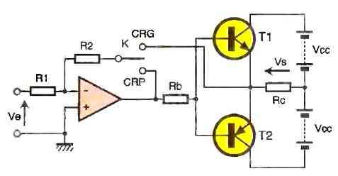
The emitter of transistor T3 is connected to the biasing circuit, which receives the output signals from the operational amplifier (OP-AMP) IC1 at its base.
The OP-AMP is set up as an inverting adder (or as an amplifier for input signals when resistor R1b is used instead of R1a).
The signal to be amplified (ve(t)) is fed to one of the inputs of IC1, while the other input receives a bias voltage that can be adjusted by Aj1.
If the function generator (GBF) that supplies this prototype produces signals with a maximum amplitude of 5V or less, these signals are amplified by a factor of 3 (R2/R1b) when the jumper switch K1 is set downwards.
When the GBF produces a signal of 10V or more, the amplification is not needed, so K1 is switched up (amplification -R2/R1a=-1).
The feedback resistor (R2) of the OP-AMP has two options: it can be directly connected to the output (jumper switch K2 down = partial feedback, CRP) or to the hot point (S) of the load resistor Rc (global feedback, CRG).
The power supply for this OP-AMP stage comes from resistors R6 and R7, which are each coupled with capacitors C3 and C4. These capacitors act as low-pass filters to smooth out any possible variations in the main high-power supply voltage. This is the summary of the specific features of this OP-AMP stage.
To prevent parasitic oscillations in the circuit, this precaution is necessary, especially when the power source has a low current limit.
Likewise, capacitors C1 and C2 with high capacitance values decouple the ±15V power lines.
To prevent high-frequency oscillations in this circuit, which has a high current gain, the capacitor C6 is connected in parallel to R4, the base resistor of T3. Diodes D4 and D5 protect the circuit from reverse polarity on the power supply.
How to Build
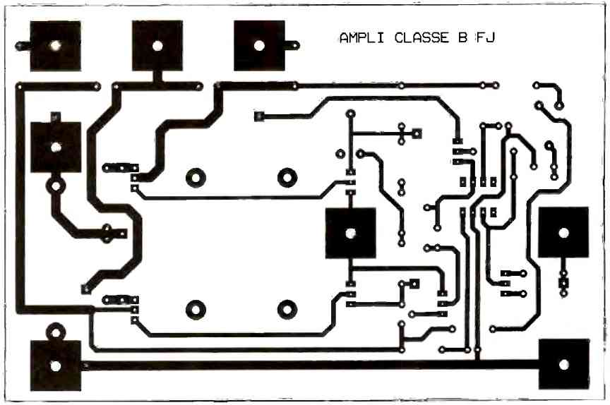
All the components of the circuit are supported by the printed circuit board (PCB), which has the layout shown in Figure 8 below.

The wiring is easy to set up; just follow the suggested layout in Figure 9 below..

To enable the structural change, we use breakable male pin headers with a 2.54 mm pitch as "switches". Each switch needs three pins. We secure the power transistor heat sinks, which are TV21 models, with screws of 3 mm diameter.
The assembly process requires careful drilling to place the transistors on these heat sinks.
To improve thermal exchange, resistors RE1, RE2, and load resistor Rc should be elevated by at least one millimeter above the PCB.
The chassis has different 4 mm female terminals that can connect to external devices, such as a function generator or a DC power supply. The circuit also has several test points (TB1, TE1, etc.) that allow the observation of signals at various locations.
How to Use
This circuit demonstrates power amplification in class B and class AB by allowing various measurements: waveforms at different circuit points and configurations, distortion levels, current consumption, output power, efficiency, and operating limits, to name a few.
Different configurations allow for various measurements, such as the following:
- Analyzing and measuring how much the output signal is distorted
- Finding the highest input level that makes at least one of the output transistors saturate
- Measuring the power output (Ps) and the power input (Pf) of the circuit
- Calculating the efficiency
To observe the signals, an oscilloscope is necessary.
Switched capacitor filter circuits, which we have explored and applied in previous months, can help measure distortion levels.
A true RMS voltmeter is needed to measure the output power (Ps) accurately, using the formula Ps = Vs²eff / Rc. This is because the output signal may not be sinusoidal, which happens with uncompensated class B amplification. The voltmeter should be connected across the load resistor (Rc).
To achieve a power of 5W at the load with a load resistor value of 10 ohms, we need an effective voltage of 7V, which corresponds to a peak value of 10V in a sinusoidal regime.
To measure the power supplied by the power sources (Pf = Vcc(I* + I)), we should insert a DC ammeter between each power source and the circuit.
The circuit's efficiency (η = Ps/Pf) can be calculated by knowing Ps and Pf.
A class B amplifier has a maximum theoretical efficiency of 78%, but this is not realistic in practice (except in cases of measurement or calculation errors).
The theoretical calculation of maximum efficiency does not account for transistor threshold voltages, non-zero Vcesat values, and the presence of emitter resistances. These factors can cause deviations from theory in practice.
The operational amplifier stage also introduces a phase shift of 180° when in use, which is normal because it functions as an inverter.
Analyzing Configurations
If you're using an op-amp IC, you should know that the DC bias from the potentiometer Aj1 can change the operating point of the power stage.
So, you need to check that the voltage Vs on the load is zero when it's not working for every configuration change.
To get the basic class B amplifier, you can set jumpers K4 and K5 towards input terminal J3. This circuit is like the one in Figure 3, but it has extra emitter resistors.
This input (J3) and the ground can be directly connected to the function generator (GBF) if it delivers a signal with an amplitude of at least 10y. To prevent the GBF signal from being coupled to the output of the operational amplifier IC1, jumper K3 should be removed or placed in the down position.
To increase the amplitude of the GBF output signal, you can connect it to input terminal J1 and move jumper K1 down to activate the amplifier.
Make sure you also move jumper K2 down (CRP) and jumper K3 up to enable the IC1 output signal to reach terminal J3.
To see how the overall feedback works (as illustrated in the diagram in Figure 10 below), you just need to shift jumper K2 up.

The output signal's shape changes a lot because of this modification. It looks distortion-free even at low levels.
The transistor starts conducting when the voltage is Vseui I/A, where A is the operational amplifier IC1's open-loop gain.
As the input voltage surpasses a few μV, transistors T1 and T2 start to conduct because A is nearly 100,000.
The conduction seems constant to the observer because this value is very small. The circuit's voltage amplification VsNe equals -R2/R1 in this particular configuration. A power operational amplifier is formed by combining the operational amplifier and the class B amplifier.
To switch from class B to class AB, you need to change the locations of jumpers K3, K4, and K5. Move the first jumper down and put the other two as far as you can from terminal J3.
Apply the signal that you want to amplify to terminal J1. To use this configuration, first adjust Aj1 until the output voltage Vs is zero when there is no input.
Next, apply a sinusoidal signal Ve(t) and see how adjusting Aj2 affects the shape of the output signal.
After compensating for the crossover distortion, you should verify the quiescent point of the output stage.
If Vs is not zero when ve(t) is zero, adjust Aj1. Also, make sure that the voltage drop across RE1 and RE2 is no more than 10 or 20mV (which means emitter currents of 10 or 20mA).
This text implies that the transistors may have improper biasing. If so, you may need to tweak Aj2, even at the cost of some output signal quality.
You can offset this minor loss by applying global feedback instead of local feedback (through K2).
A configuration change requires readjusting the quiescent point of the output stage with Aj1.
Otherwise, transistors T1 and T2 could overheat, even if there is no signal at the circuit input.
The purpose of these guidelines is to explain how different configurations can benefit users in different ways and to clarify how class B and class AB power amplifiers work.