
The IC 4017, IC 4093, and IC 4013 may be used to construct several straightforward yet efficient electrical toggle flip flop switch circuits. I will examine the manner in which these may be used to activate and deactivate a relay, which may subsequently be used to turn on and off an electrical load—a fan, lights, or other such appliance—with only a single push of a pushbutton.
Understand Flip Flop Circuit
A bistable circuit, consisting of two stable phases that may be either ON or OFF, is the basis for how a flip flop relay circuit operates.
In real-world circuits, it enables an associated load to respond to an outside ON/OFF switching signal by alternately toggling between an ON and an OFF state.
I will be demonstrating how to build flip-flop relay circuits depending on the 4017 and 4093 integrated circuits in the illustrations that follow.
These have the ability to react to different triggers by means of a push button, therefore switching a relay and a load through an ON to an OFF condition and the other way around.
The circuit may be modified to reliably switch between consecutive input triggers, in two ways manually or electrically, through the addition of a small number of additional passive components.
These can be controlled either electronically or manually by use of externally generated triggers.
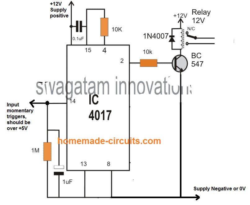
IC 4017-Based Practical Electronic Flip-Flop Switch Circuit
The first concept describes a practical flip-flop toggle switch circuit based on the IC 4017. In this section, you'll find very few components, and the output is usually satisfactory.
With reference to the image, we can observe that the integrated circuit is connected according to its conventional design, meaning that a logic high at its output is shifting across pins as a result of the applied clock at pin # 14.
This converts the alternative switching at its clock input—which is identified as clock pulses—into the necessary flipping at its output pins. The next points can help you understand the entire working:

Parts List
All parts are standard version, no special specs:
| Part | Value/Specification |
|---|---|
| R4 | 10K |
| R5 | 100K |
| R6, R7 | 4K7 |
| C6, C7 | 10µF/25V |
| C8 | 1000µF/25V |
| C10 | 0.1µF, DISC |
| Diodes | 1N4007 |
| IC | 4017 |
| T1 | BC 547 |
| T2 | BC 557 |
| IC2 | 7812 |
| Transformer | 0-12V, 500mA, INPUT AS PER AREA SPECIFICATIONS |
Working Explanation
The output pins of the IC 4017 are known to be progressively flipped high from # 3 to # 11 in the following order: 3, 4, 2, 7, 1, 5, 6, 9, 10, and 11. This is in reaction to each logic high pulse at pin #14.
But, by hooking up any of the aforementioned pins to reset pin #15, you may halt this process at any time and start over.
For instance, in this particular case, pin #4 of the integrated circuit is linked to pin #15, meaning that whenever the sequence of events (logic High) approaches pin #4, this shall be halted then resumed to pin #3, repeating the cycle.
All it indicates is that the sequence typically alternates back and forth between pins 3 and 2, which is a standard switching operation.
The following explanation may help you better understand how this electrical toggle switch circuit operates:
Pin # 14 of the IC is pulled down to ground each time a positive trigger is hooked up to the base of T1. As a result, the IC enters a state of standby.
T1 ceases conducting the second the trigger is withdrawn, and pin # 14 now immediately gets a positive pulse from R1.
The integrated circuit (IC) promptly flips its output from pin #3 to pin #2 after recognizing this as a clock signal.
The output transfers from pin #2 to pin #4 in response to the subsequent pulse, which has the identical outcome. However, as pin #4 is linked to reset pin #15, as previously mentioned, the condition restores to pin #3 (the original position).
As a result, the process is carried out once again each time T1 is triggered—either by hand or by an external circuit.
Enhancing the circuit to manage multiple loads
We're going to now examine methods to enhance the IC 4017 design mentioned above so that it may control 10 potential electrical loads with a single push button.
Mr. Russell Arnold requested the concept. The following is a list of the specifications:
Circuit Goals and Specifications
Every step listed below must be carried out in accordance with the diagram below.
As soon as AC switch S1 is initially turned ON, AC load 1 should turn ON and remain in an ON state until S1 is turned OFF. AC load 2 should not be turned on while doing this.
Once S1 is turned on yet again, AC Load 2 should turn on and remain on until S1 is turned off. AC load 1 should not be turned on while doing this.
Once S1 is turned on for the third time, the two AC loads should turn on and remain on until S1 is turned off.4. The steps 1, 2, and 3 of the process of operation should be repeated the fourth time the S1 is turned ON.

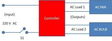
I want to utilize the above layout in my rental apartment's single living room. The fan is in the middle of the roof, and the chamber contains hidden wiring.
As the main light in the room, the illumination is going to be linked in line with the fan. The middle of the roof does not have an additional power outlet. The ceiling fan is the only accessible outlet.
Independent cables from the switchboard to the central light is not something I want to do. Therefore, I had the idea to create a logical circuit that could determine if the power supply was on or off and switch loads appropriately.
I don't want to always have the fan on when utilizing the central light, or the other way around.
The circuit should operate in accordance with its last known condition each time it is turned on.
Designing the Circuit
Without using an MCU, the straightforward electrical switch circuit below is modified to carry out the aforementioned tasks.
The associated lamp and fan are sequentially switched on by a bell push-button style switch.
The circuit explanation is simple to understand; nevertheless, should you have any questions, do feel comfortable to ask via comments below.

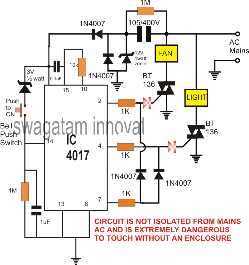
Push Button Operated Electronic Switch
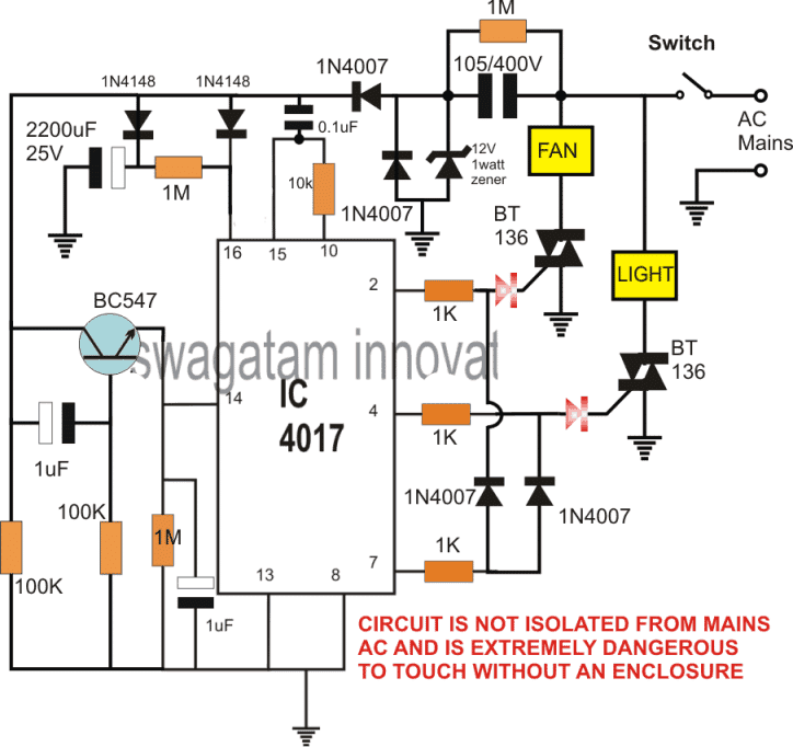
In accordance with the request and comments previously mentioned, the schematic mentioned above may be altered to function without a push button by utilizing the ON/OFF switch that is now located at the primary input side to generate the desired toggling sequences.
The revised design is shown in the following figure:

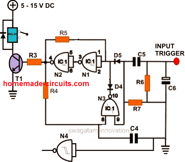
With just one IC 4093, it is possible to construct a second intriguing ON/OFF relay utilizing a single button. Let us study the steps using the description that follows.
Use IC 4093 to Create a Reliable CMOS Flip-Flop Circuit

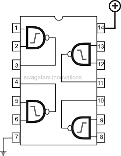
IC4093 Pinout Details

Parts List
| Part | Value/Specification |
|---|---|
| R3 | 10K |
| R4, R5 | 2M2 |
| R6, R7 | 39K |
| C4, C5 | 0.22µF, DISC |
| C6 | 100µF/25V |
| D4, D5 | 1N4148 |
| T1 | BC 547 |
| IC | 4093 |
The next idea involves creating a fairly precise circuit with IC 4093's three gates. The image illustrates how the inputs of N1 and N2 are combined to create logic inverters, which function similarly to NOT gates.
This implies that any amount of logic utilized to their inputs will result in an inverted output. Moreover, a feedback channel via R5 connects these two gates in series to provide a latch arrangement.
As soon as N1 or N2 detects a positive trigger at its input, both of them will latch immediately. Essentially, the purpose of adding gate N3 is to periodically release this latch soon after each newly generated input pulse.
A brief description will help you better understand how the circuit operates:
Working Details:
N1 reacts fast to a pulse at the trigger input, switching the status of its output and causing N2 to do the same.
As a result, N2's output rises, feeding feedback to N1's input through R5, causing the two gates to latch in that configuration.
The relay and the attached load are activated by the previous control circuit while the output of N2 is locked at logic high.
Additionally, the high output gradually charges C4, causing one of gate N3's inputs to turn high. R7 is currently holding the second N3 input at logic low.
This input is going to temporarily go high in response to a pulse at the trigger point, driving its output to dip low. This is going to immediately eliminate the latch by pulling the input of N1 to ground via D4.
As a result, the N2 output will decrease, thereby deactivating the relay and the transistor. At this point, the circuit has returned to its initial condition, the process may be repeated from the next input trigger onward.
Using IC 4013, create a flip-flop circuit
The ease of access to numerous CMOS integrated circuits (ICs) has simplified the process of constructing intricate circuits, and novice circuit builders are undoubtedly having fun creating circuits using these amazing ICs.
IC 4013 is a particular kind of device that could be used separately to carry out the suggested tasks. It functions essentially as a dual D-type flip flop integrated circuit.
To put it briefly, the integrated circuit (IC) has two modules that may be readily designed to function as flip flops simply simply incorporating some passive external components.
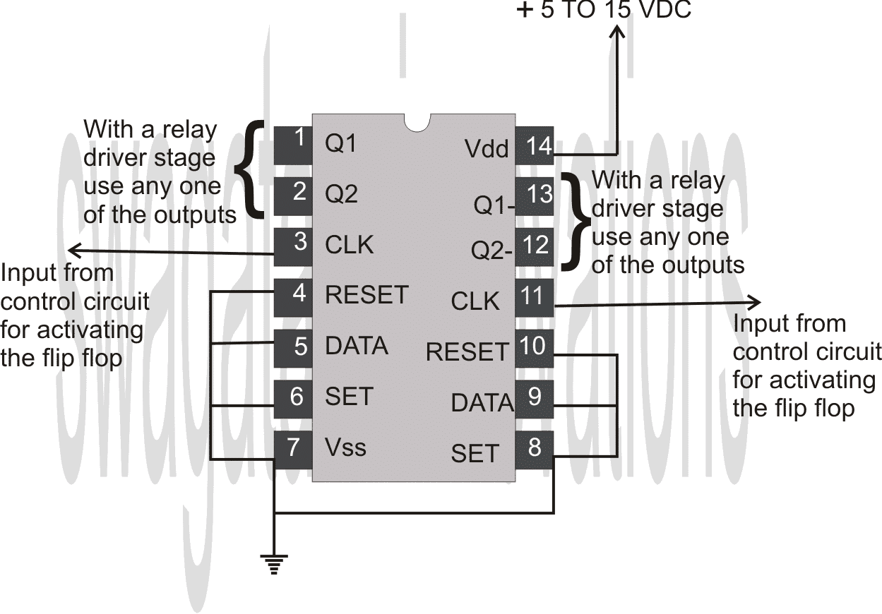
IC 4013 Pinout Specifications
The next few points can help us understand the IC.
The pinouts of each individual flip-flop module are as follows:
Q and Q-dash are complementary outputs.
CLK stands for clock input.
Data: The unnecessary pin out has to be linked to either the positive or negative supply line.
SET and RESET: These are complementing pinouts that are used to either set or reset the output conditions.
The set/reset or clock pinout inputs cause the outputs Q and Q-dash to sequentially transition between their logic states.
for as long as the clocks continue to run, applying a clock frequency at the CLK input causes the output Q and Qdash to successively switch states.
In a same manner, the set or reset pins are capable of being manually pulsed with a positive voltage source to alter the Q and Qdash state.
When not in use, the reset pin and the set should always be linked to ground.
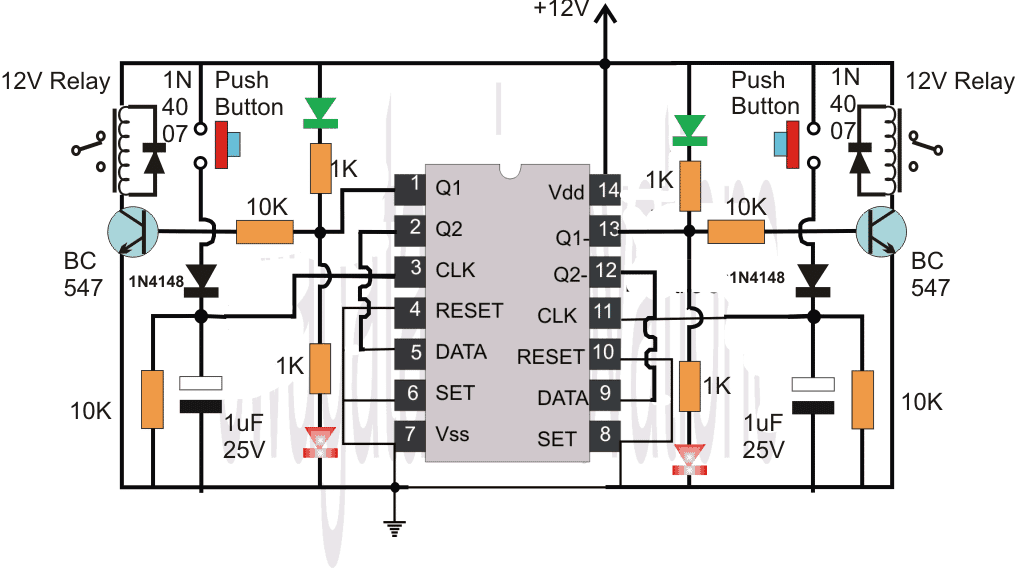
A basic IC 4013 configuration that may be utilized as a flip flop circuit and used to achieve the desired objectives is shown in the circuit diagram below.
When just one of them is being employed, ensure that the set/reset/data and clock pins of the other portion that isn't in use are grounded properly. Both can be utilized if necessary.
Here is a representation of a flip flop circuit used in real-world applications utilizing the 4013 IC that was previously presented.

Memory and Backup for the Flip Flp Circuit in Case of Mains Failure
The 4013 architecture described above may be upgraded with a capacitor recovery, as seen in the accompanying picture, if you would want to incorporate a mains electricity breakdown memory and backup capability.

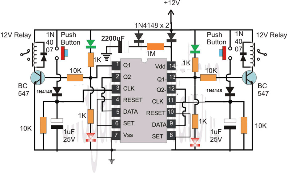
It is evident that a high-value capacitor and resistor network are connected to the IC's supply terminal, along with a few diodes, to guarantee that the capacitor's stored energy is utilized exclusively to power the IC and not any other external stages.
In the event of a mains electrical failure, the 2200 uF capacitor keeps the integrated circuit's "memory alive" by gradually releasing the energy it has stored to the supply pin, ensuring that the IC remembers the latch position even in the absence of mains power.
Relays are kept from forgetting the earlier switch ON condition throughout the mains' failure by the IC, which provides the initially configured latching operation on the relay in accordance with the prior scenario as soon as the mains restores.
IC 741 is used in an SPDT electronic 220V toggle switch.
An apparatus that alternately turns an electrical circuit ON and OFF as needed is called a toggle switch.
When electrical switching is needed, mechanical switches are often utilized for these kinds of tasks.
One significant disadvantage of mechanical switches is that these devices are susceptible to deterioration and damage, arcing, and radio frequency noise.
These procedures can be replaced by an electronic version using a straightforward circuit that is described here. An intriguing electrical toggle switch may be constructed and utilized for its intended application with just one operational amplifier and a few additional inexpensive passive components.

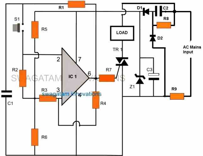
Even though the circuit additionally incorporates a mechanical input device, the suggested toggling motions are only implemented by alternating pushes on the small micro switch.
Because a micro switch is extremely adaptable and highly resilient to mechanical stress, it has no effect on the circuit's efficiency.
Circuit Working
With a 741 opamp serving as the primary component, the schematic seen in the image illustrates a simple electrical toggle switch.
Because the integrated circuit is designed to function as a high gain amplifier, the signal it produces has a propensity to be readily activated to logic 0 or 1, respectively.
A small amount of the output voltage is sent back into the opamp's non-inverting input.
As soon as the push button is depressed, C1 is connected to the opamp's inverting input.
The opamp switches state instantly, assuming that the output was at logic 0.
At this point, C1 starts charging via R1.
On the other hand, holding the switch down for an extended length of time will only partially charge C1, and it is only when the switch is removed that C1 starts to charge and keeps charging until it reaches the supply voltage threshold.
C1 has now become unconnected since the switch is open, which enables it to "retain" the output data.
The completely charged C1's high output is now accessible at the op amp's inverting input whenever the switch is clicked again. The op amp subsequently changes states and generates a logic 0 at the output, causing C1 to begin discharging and returning the circuit to its initial state.
After the restoration of the circuit, the cyclical process above can begin again.
In order to react to the outputs of the opamp for the pertinent switching operations of the associated load, a conventional triac trigger arrangement is utilized as the output.
Parts List
| Component (all resistors are 1/4W 5%) | Value/Specification |
|---|---|
| R1, R8 | 1M |
| R2, R3, R5, R6 | 10K |
| R4 | 220K |
| R7 | 1K |
| R9 | 22 ohm 2 watt |
| C1 | 0.1uF |
| C2, C3 | 470uF/25V |
| S1 | Micro-switch Push Button |
| IC1 | 741 |
| Triac | BT136 |
| D1, D2 | 1N4007 Diodes |
Utilizing Set/Reset Touch Pads for IC 741 Flip Flop

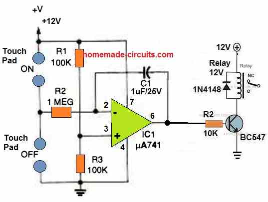
By applying a pair of touch pads, a 741 IC may also be exploited to build a set/reset type flip flop circuit.
Relay driver stage and load can both be turned on by using the upper pair of touch pads to activate the 741 output, as depicted in the above figure.
Touching the lower pair of touch pads causes the IC 741 to reset to its initial state, which turns off the relay driver stage's output.
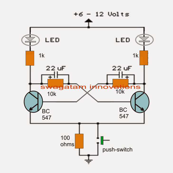
Flip Flop Circuit using Transistors
The next flip flop design teaches us how to create a few transistorized flip flop circuits that may be used to turn a load on or off using just one push button trigger.
An alternative term for such devices is transistor bistable circuits.
Transistor bistable corresponds to a circuit state in which the circuit responds to an incoming trigger to make itself stable (indefinitely) between two states: ON and OFF; the word "bistable" describes to this stable state depending on one of the two states.
A digital voltage trigger input or an electrical push button may often be used to alternatively turn the circuit ON and OFF steadily.
Through the aid of the following two circuit illustrations, we'll comprehend the recommended bistable transistor circuits:
How the Circuit Operates
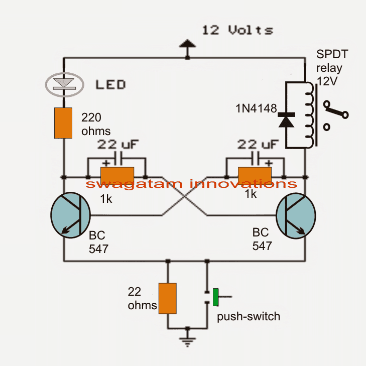
An deliberately omitted base to positive resistor makes the first image of a straightforward cross-coupled transistor circuit resemble a monostable multivibrator arrangement.
Comprehending the bistable behavior of transistors is rather simple.
When the power is turned on, one transistor would fully turn on while the second will fully turn off, based on the tiny unbalance in the component values and transistor characteristics.
Assuming the right side transistor conducts first, the biasing for it comes from the left side LED, 1k, and 22uF capacitor.
The left transistor would entirely turn off soon after the right transistor has fully switched on because the 10k resistor placed across the collector/emitter of the right transistor will now hold the base of the left transistor grounded.
for as long as the circuit is powered on or until the push-to-ON switch presses down, the aforementioned position will remain firm and irreversible.
The left-hand 22 uF capacitor will now be completely charged and won't respond when the indicated push button is temporarily pressed.
But, because the right-hand 22uF is discharged, it will have more freedom to conduct thus offering the left-hand transistor a stronger bias, causing it to quickly flip ON and turn the situation around such that the right-hand transistor is forced to turn off.
Until the push button is touched again, the previously held position continues to stay in place. By temporarily activating the push switch, the toggle position may be switched alternatingly from the left to the right transistor and vice versa.
Whichever transistor is made operational by the bistable actions will cause the corresponding LEDs to light up alternately.
Circuit Diagram

Adding a Relay to the Transistor bistable flip-flop circuit
The aforementioned example taught us how to enable the bistable latching of a few transistors in order to toggle the necessary indicators and pertinent LEDs by only pushing one push button.
Switching a relay is often necessary if one wants to switch larger external loads.
With a few simple adjustments, the circuit described above may be used to turn a relay ON or OFF.
The circuit is essentially the same as the previous transistor bistable setup when we examine the resistor values and the relay that has been added in place of the right-hand LED. Additionally, the resistor values have been slightly changed to allow for any additional current that might be needed for the relay to activate.
Additionally, the circuit operates in the same way.
Contingent on the circuit's original state, pushing the switch will result in turning the relay ON or OFF.
By repeatedly pushing the push button that is linked to the relay, you may flick it from an ON to an OFF state and toggle the external load that is hooked up to the relay contacts correspondingly.
Bistable Flip Flop Image
Using the IC 4027 to Make a Flip Flop Circuit
once the touch-finger pad has been touched. The pnp transistor T1 starts to function. Because of CI and C2, the resulting pulse at the input clock of the 4027 has extremely lagging edges.

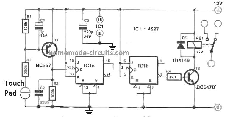
As a result, (and amazingly) the first J-K flip-flop in 4027 acts as a Schmitt control gate, converting the extremely slow pulse at its input (pin 13) into a steady electrical signal which could be fed to the clock input (pin 3) of the subsequent flip-flop.
Later on, as described in the guide, the second flip-flop produces an actual switching signal that may be utilized to turn a relay on or off via a transistor stage, T2.
You can touch the contact plate using your finger to get the relay to conduct alternatively.
Relays use a maximum of one mA of circuit current while they are off and up to 50 mA when they are active. So long as the coil voltage is 12 V, any less expensive relay could be utilized.
When using a relay to control a mains equipment, however, be sure the connections are appropriately rated.
Using IC 4049 for making a Flip Flop

Set-Reset Flip Flop Using IC 4011
CMOS integrated circuits offer multiple advantages over TTL. The high input impedance is one of the important characteristics. A flipflop is created in the accompanying diagram by connecting two NOR gates in a cross-coupled manner across one another.
Ambient noise causes an AC voltage to arise at the G1 input whenever touch panel S is touched. The flipflop sets, turning on the relay RLA1, when the G1 output becomes negative during the first positive cycle. For as long as neither the R plate nor the RESET plate are touched, the situation will persist.
R1 and R2 must not be eliminated because they quickly discharge any voltage levels that are created on the plates in response to contact, allowing the flipflop to change states quickly.

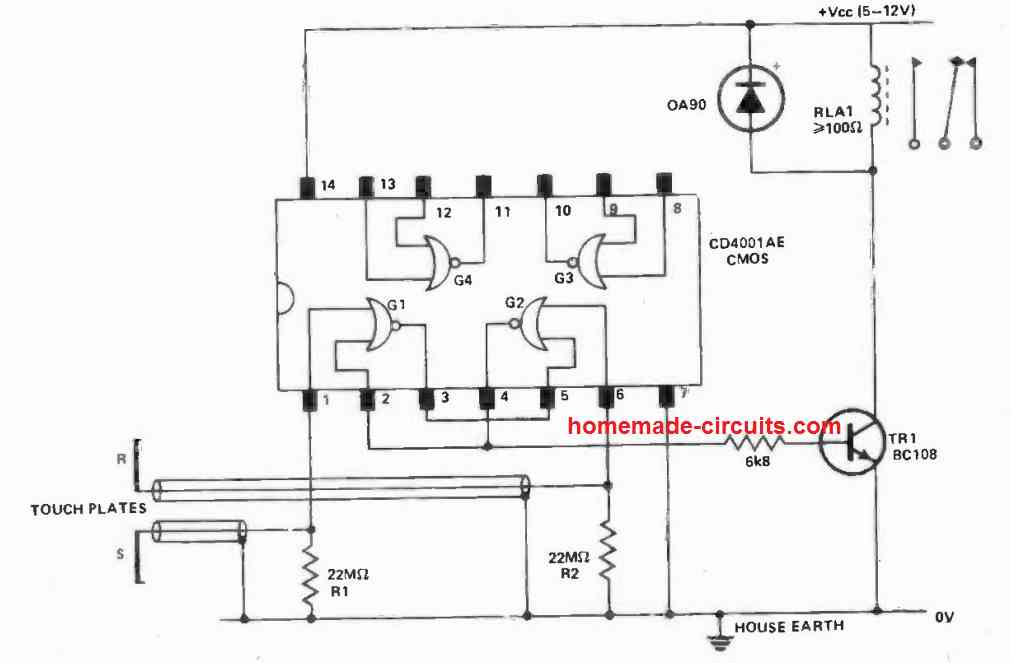
Furthermore, whenever the supply is unplugged, R1 and R2 guard against any static charges building up that might harm the IC.
Since 22 m Ohm resistors might be difficult to find, two 10 m Ohm resistors could be coupled in series instead.
As there is no current wasted in the relay off state while a milliammeter is used, the flip flop circuit might be maintained switched ON constantly.
Relay TR 1 collector becomes a TTL output with a high fan out if relay RLA1 is omitted.
In the event that G3 and G4 are not in use, connect their inputs to ground. Provided the connecting wires are terminated with a shield, the touch plates can be placed a few feet far from the integrated circuit.
Some Other Flip Flop and Set/Reset Circuits
A couple additional simple flip-flop circuits that utilize CMOS gates and an operational amplifier are explained in the sections that follow.
In the first circuit, an IC 4050 single buffer gate is used. The IC 4011 is used in the second circuit by a few gates.
Using a Single Buffer gate
With a single buffer gate, like the one from the IC 4050, it is straightforward to construct a flip flop or set reset circuit.

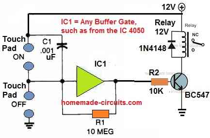
The suggested flip flop circuit may be configured with a handful of touch pads and a 10 M resistor, as seen in the above image.
The flip flop's output is connected to a relay driver stage, which turns the load on or off in accordance with the finger contact.
Using Two NAND Gates for making a Set-Reset Switch

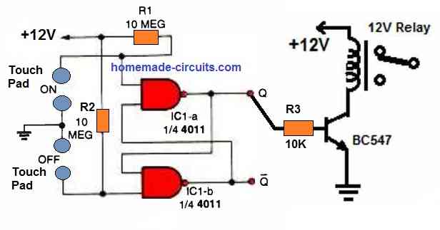
With only a few NAND gates from an integrated circuit (IC) like the 4011, anyone can quickly construct the charming little set/reset flip flop circuit seen in the upper diagram.
The flip flop is set when the top pair of touch pads is touched, turning on the relay driver.
The flip flop is reset when the bottom pair of touch pads is touched, turning off the relay driver.
Note: In order to protect the transistor, be sure to put a freewheeling diode across the relay coil.
A Single 4011 IC to make a Set/Reset Flip Flop
The next circuit could work perfectly for you if you choose not to utilize two separate sets of touch pads and are seeking for a flip flop set/reset circuit utilizing only one set.

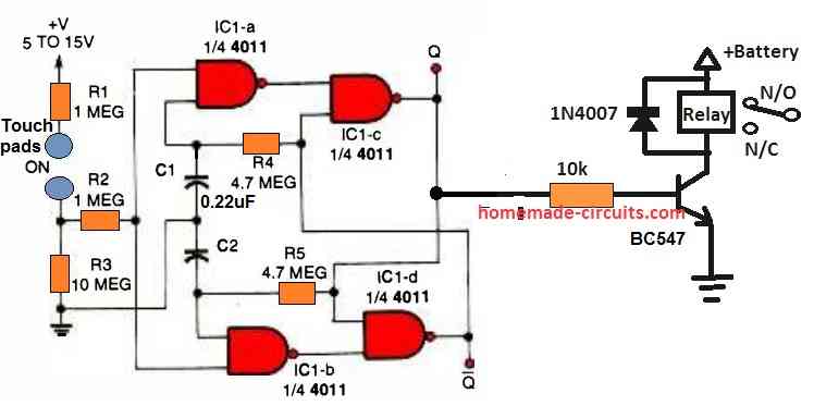
A set/reset operation is created across the outputs whenever the touch pads are repeatedly pressed and set free, causing the outputs Q and Q-bar to concurrently toggle high and low. In line with it, the relay driver stage can be turned ON and off.