
This article will teach you how to construct discrete transistor logic gates for NOT, AND, NAND, OR, and NOR. Transistor logic gates have BJT the primary benefit of operating at voltages that are as low as 1.5 V.
The voltage that is obtainable in some electrical applications might not be sufficient to power TTL or even CMOS ICs. This is particularly valid for battery-operated devices. Without a doubt, the 3-volt logic IC option is always available. They do not function below their specified voltage requirements though, therefore are not often readily available to enthusiasts or experimenters (typically under 2.5 volts DC).
In addition, a battery-powered product could only be able to accommodate one 1.5-volt battery. So, what will you do in that situation? Transistorized logic gates are often able to substitute integrated circuit logic gates. Only one transistor is usually needed for a normal NOT gate inverter logic, and only a few transistors are usually needed for any specific logic gate.
Why Transistorized Logic Gates are Better
The following is a summary of the primary benefits of transistor-based logic gates:
ICs are more expensive than transistors.
Logic gates that are transistorized may function at voltages as low as 1.5 V, but their integrated circuit counterparts require a minimum of 3 V.
An IC-based logic gate cannot be specifically tailored to regulate larger loads, but a transistorized logic gate can.
Field Effect Transistor vs Bipolar Transistor
Which is a preferable alternative for low-voltage transistorized logic circuits: bipolar transistors or field effect transistors (FETs)? FETs' extremely low "on" resistance is one of their best qualities. They also require extremely low gate-turn-on current.
They do have a drawback, though, in very low-voltage situations. The gate voltage range tends to be one volt or such. If a pull-down or current-limiting resistor is connected to the gate, the permitted voltage could fall beneath the FET's ideal operating range.
On the other hand, since bipolar transistors just need 0.6 to 0.7 volts to turn on, these offer a benefit in exceptionally low voltage, single battery applications.
Additionally, most popular FETs—which are typically available in bubble packs at your local electronics store—are frequently more expensive than bipolar transistors. Furthermore, a whole bundle of bipolar transistors may often be bought for the same price as two FETs.
Managing FETs requires much more caution than managing bipolar transistors. FETs are especially vulnerable to breakdown from electrostatic discharge and ordinary experimental usage. A fun, inventive weekend of experimenting or invention might be ruined by burned components, not to mention the psychological suffering of troubleshooting.
Bipolar Transistor Basic Working
Bipolar NPN transistors are used in the logic circuit examples described in this write-up given that these devices are inexpensive and don't require specific care. Prior to completing your circuit, suitable precautions must be followed to prevent harm to the device or the components that are supporting it.
Though the main components of our circuits are Bipolar Junction Transistors (BJTs), FET electronics could have been used just as well.
One of the simplest designs is the basic switch circuit, which is a straightforward transistor application.
Making a BJT NOT Gate

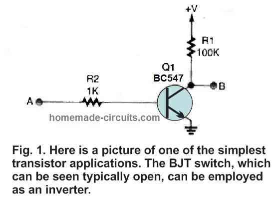
Figure 1 displays a schematic of the BJT switch. The switch can be interpreted as being maintained low or typically open, according upon the way it is used in an individual application.
With point A as the input, the basic switch circuit in Fig. 1 may be used to produce a basic NOT gate inverter logic gate. A NOT gate functions by providing a high or logic 1 (equivalent to the V+ level) at the output (point B) if no DC bias is applied to the transistor's base (point A; Q1).
The output of the circuit is pushed low, or to logic 0 (roughly identical to zero voltage), once the transistor turns ON and the correct bias is applied to Q1's base. A universal bipolar transistors, often known as BC547s, are the type of transistor Q1 is. They are mostly used in low-power switching and converter applications.
All analogous transistors, including the 2N2222, 2N4401, and so on, may function. A balance across interoperability and low current drain was achieved by choosing the values of R1 and R2. Resistors are 1/4 watt, 5% units used in all designs.
Between 1.4 and 6 volts DC, the supply voltage can be changed. Be aware that if the load resistor and output connector are moved to the transistor's emitter it can be used to operate like a buffer.
Buffer Gate using BC547 BJT

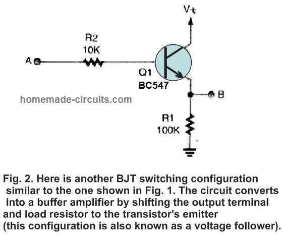
Similar to the setup in Figure 2, a voltage follower, also known as a buffer amplifier, is a kind of logic switching architecture. The configuration shown here differs from the one in Fig. 1 primarily in that the load resistor and output wire are both moved from the transistor's collector to its emitter.
Through repositioning the output terminal and load resistor to the opposite side of the BJT, the transistor's operation can be additionally "reversed".
That is to say, while the circuit's input is not biased, the circuit's output stays low; once the circuit's input is biased with a sufficient voltage, the circuit's output rises. (The fact that it is the absolute reverse from what occurred in the previous circuit.)
BJT Two-Input Logic Gate
AND Gate using Two Transistors

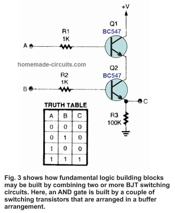
The truth table for a simple two-input AND gate and its construction with two buffers are shown in Figure 3. The output outcomes for every distinctive combination of inputs are shown in the truth table. Point C functions as the circuit's output, while points A and B are utilized as its inputs.
The truth table shows that a logic-high output signal is produced by one particular set of input variables, while a logic-low output is produced by all other input combinations. After turning into high, the AND gate's output in Figure 3 stays marginally below V+.
The voltage drop across both of the devices (Q1 and Q2) is the reason of this.
2 BJT NAND Gate Circuit
Figure 4 displays an additional version of the circuit from Figure 3 along with the corresponding truth table. By moving the output (point C) and output resistor to the collector of the higher transistor (Q1), the circuit becomes a NAND gate.

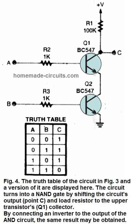
In order to draw the low side of R1 to ground, each Q1 and Q2 must be turned ON, which negates the voltage loss at output C.
Additional transistors might be linked in the layouts above to give three, four, etc. input AND or NAND gates if the transistor AND or transistor NAND gates require a few additional inputs.
V+ must be boosted appropriately, though, to make up for the voltage impairments of each of the transistors.
2 BJT OR Gate
Figure 5 displays the truth table for the OR-gate circuit in addition to a different type of logic circuit using 2 inputs.

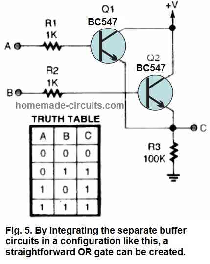
When any input A or input B gets turned high, the circuit's output becomes high; nevertheless, the voltage drop is more than 0.5 volts because of the cascading transistors. Once more, the numbers demonstrate that the system has sufficient voltage and current to run the transistor gate that follows.
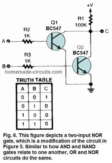
2 BJT NOR Gate Circuit
The following gate on our list, a two-input NOR gate, is shown in Figure 6 along with its truth table. OR and NOR circuits react to each other in a manner akin to that of AND and NAND gates.

Every gate indicated has the capacity to provide sufficient power to open one or more neighboring transistor gates.
How to Implement Transistor Logic Gates
With the previously described digital circuits you happen to now own, what are you going to do? Everything that might be achieved without being concerned regarding supply voltage constraints using standard TTL or CMOS gates. Following are some examples of real-world uses for transistor-logic gates.
Demultiplexer Circuit
Figure 7 shows a 1-of-2 demultiplexer featuring two NAND circuits and 3 NOT gates. The driving signal is supplied to the circuit through the DATA input, and the proper output is selected through the one-bit "address input," which might be between OUTPUT1 or OUTPUT2.

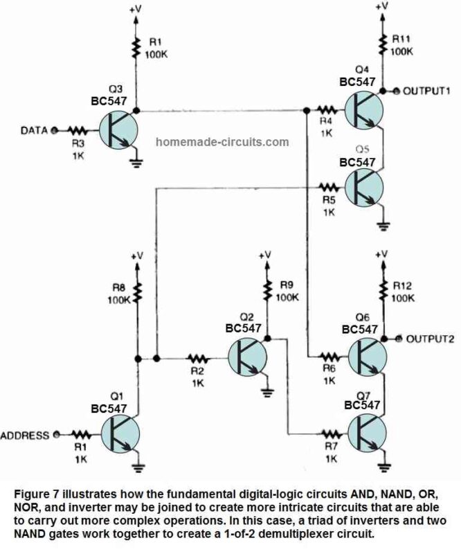
Provided the data frequency is kept below 10 kHz, the circuit performs at its best. The operation of the circuit is simple. The necessary command is given to the DATA input, turning on Q3 and inverting the data that comes in at Q3's collector.
Once the ADDRESS input gets low (grounded or a zero signal is delivered), Q1's output is pushed high. The high output of the Q1 is split into two pathways at the collector. Q1's output is sent to Q5's base (that's one of a two-input NAND gate's legs) along the first route, turning on Q5 and consequently "activating" the NAND gate composed of Q4 and Q5.
The high output of Q1 is concurrently sent into the input of a different NOT gate (Q2) in the second route. Q2 goes through a twofold inversion before its output becomes low. The NAND circuit is turned off when this low is provided to Q7's base, which is one terminal of a second NAND gate composed of Q6 and Q7.
In these cases, any data or signal provided to the DATA input ends up at OUTPUT1. On the other hand, if a high signal is applied to the ADDRESS input, the circumstances are the opposite. This means that since the Q4/Q5 NAND gate is deactivated and the Q6/Q7 NAND gate is enabled, any data supplied to the circuit will appear at OUTPUT2.
Oscillator and Clock Generator
The transistor logic gate application that follows is seen in Figure 8. It is a simple oscillator or clock generator that consists of 3 regular NOT gate inverters, the first of which is controlled by a feedback resistor, R2, placing it in the analogue section.

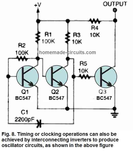
A third NOT gate (Q3) supplying the counterpart of the oscillator output is provided in order to level off the output. The frequency that is used of the circuit may be altered by adjusting the C1 value. With the stated part numbers, the output signal exhibits an average frequency of approximately seven kHz and V+ at 1.5 volts DC.
RS Latch Circuit
This last application circuit, an RS latch composed of two separate NOR gates, is shown in Fig. 9. Resistors R3 and R4 are set to 1k ohms to provide a robust output supply at the Q and Q outputs.

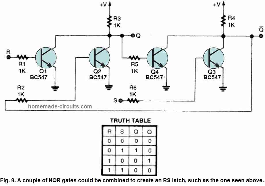
The schematic layout and truth table for the RS latch are shown. These could be only a few examples of the numerous reliable, low-voltage, digital, logic-gate circuits which could possibly be constructed from just one transistor.