
Using just one IC 555 in addition to a few additional passive components, we will learn how to create a simple DC to DC voltage doubler circuits in the following paragraphs.
The following text will assist you in understanding the specifics and building a prototype yourself if you're curious about how a basic IC 555 may be utilized to create a potent voltage doubler circuit.
About Voltage Doubler Circuits
An oscillator circuit supplies a high frequency voltage to a specifically designed resistor-capacitor connection in a voltage doubler circuit, producing an output DC that is twice as high as the input source DC.
For your convenience, there is an excellent article on our website that goes into great detail on the various voltage multiplier circuits, if you are unfamiliar with the voltage doubler idea and would like to learn more about it.
The voltage multiplier idea, commonly known as the Cockcroft–Walton (CW) generator, was initially conceptualized and applied in practice by British and Irish scientists John Douglas Cockcroft and Ernest Thomas Sinton Walton.
This article provides an excellent illustration of a voltage multiplier design by using the idea of producing ionized air to clean the air in houses.
Another type of voltage multiplier is a voltage doubler circuit, in which the output voltage can be equal to two times the supply voltage by limiting the diode/capacitor stage to only one or two stages.
An oscillator circuit is necessary to get the results you want because all voltage multiplier circuits demand either an AC input or a pulsing input.
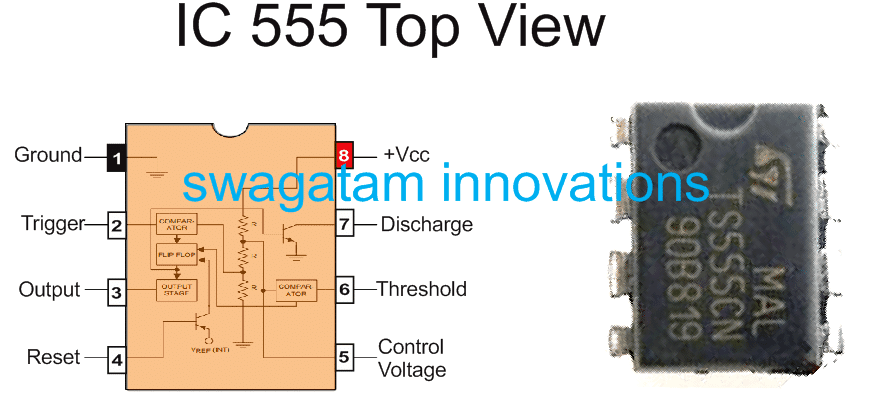
IC 555 Pin Description

An example circuit diagram for a basic IC 555 voltage doubler

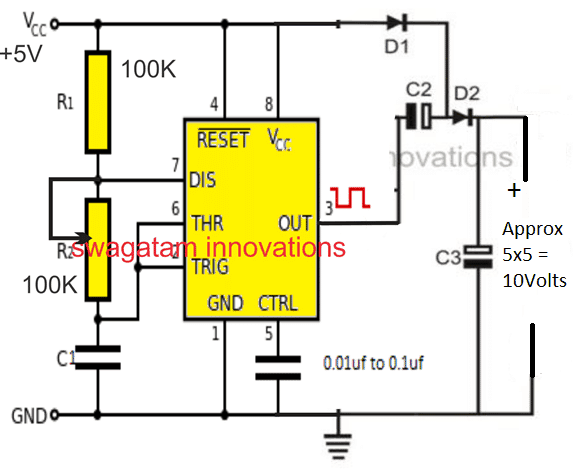
In the scenario described above, an IC 555 circuit is set up as an astable multivibrator stage, that is essentially an oscillator, with the goal of producing a pulsing DC (ON/OFF) at pin #3.
As you may remember, we already covered a voltage doubler circuit in our discussion of an LED torch circuit on this page. However, the oscillator part was constructed using IC 4049 gates.
In essence, the voltage doubling function may be obtained by substituting any other oscillator circuit for the IC 555 step.
The IC 555 can produce a greater current compared to virtually any other IC-based oscillator circuit without the need for an extra current amplifier step, hence employing it provides a little advantage.
Voltage Doubler Circuit Working
The following graphic illustrates how the D1, D2, C2, and C3 stages, that are set up as a half-bridge 2-stage voltage multiplier system, carry out the real-world voltage multiplication.
It can be a bit challenging to simulate this step in reaction to the IC 555's pin#3 scenario, and I'm still having trouble getting it to function properly in my head.
According to my brain simulation, the factors that follow may be used to illustrate how the voltage doubler step indicated above operates:
D1 can charge C2 when the IC output pin #3 is at its low logic or ground level because it can become forward biased via C2 and pin #3's negative potential. D1 and D2 can likewise concurrently charge C3 at the same time.
immediately as pin #3 reaches a positive supply voltage or high logic in the next instant, things start getting a little unclear.
Since D1 cannot discharge C2 in this situation, we further have a supply levels output through D1, C2, and C3.
The stored voltage within C2 and the positive from D1 are meant to merge with the output of C3 at that moment to create a twofold voltage, according to many other websites; yet, that is meaningless.
Kindly be sure to provide a more thorough or technologically precise argument in your comments should you have one.
How much Current?
The largest peak current may be anticipated to be at this 200 mA level as Pin #3 of the IC is designated to produce in excess of 200 mA of current; nevertheless the peak current are going to decrease based on the C2, C3 quantities.
A wider current flow across the output may be possible with bigger capacitors, thus be certain to choose C2 and C3 values judiciously. Approximately 100uF/25V will be sufficient.
A Real Working Design
While there are several electrical circuit uses for voltage doubler circuits, one possible hobby purpose would be to light a high voltage LED using a low voltage source, as seen below:

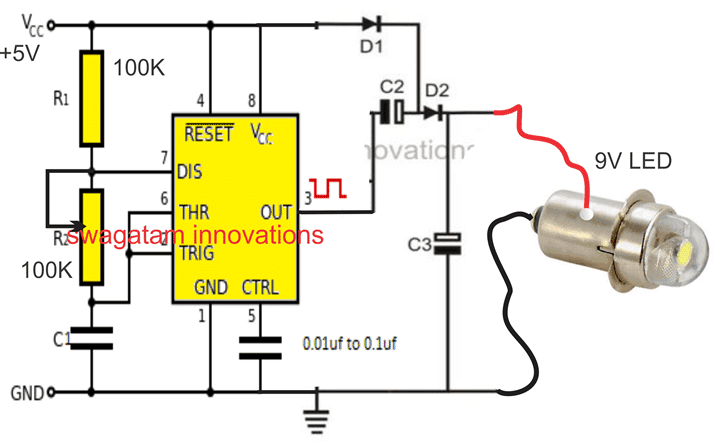
The circuit used to illuminate a 9V LED bulb through a 5V power source is shown in the circuit diagram above. This wouldn't be feasible if the 5V was supplied immediately to the LED.
The relationship between PWM, frequency, and output voltage level
Any kind of voltage doubler circuit's frequency is not very important, nonetheless a higher frequency is going to produce superior outcomes compared to a lower frequency.
A duty cycle of around 50% is appropriate for the PWM range. Narrower pulses will result in less current at the output, while too broad pulses will prevent the essential capacitors from discharging to their full potential, which will once again contribute to an inefficient output power.
The resistor R1, which determines the frequency together with the capacitor C1, can be any value between 10K and 100K in the IC 555 astable circuit under discussion. As a result, C1 can be somewhere from 50nF to 0.5uF.
Since R2 is going to provide you control over the PWM, one could employ a 100K pot to turn this into an adjustable resistance.
An Alternate 555 Voltage Doubler
This next circuit, that generates a DC output voltage that's almost twice the supply voltage, is also an IC 555 powered DC voltage-doubler.

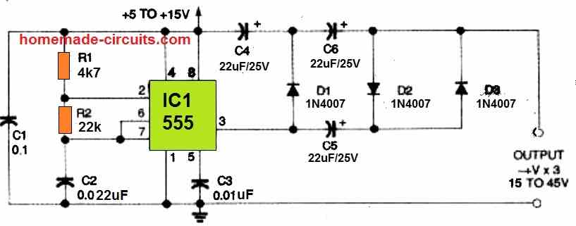
A voltage-doubler circuit made up of diodes D1 and D2, capacitors C4 and C5, and capacitors C5 is linked to the 555's output.
The circuit produces an output that is roughly double the source voltage when the output is empty. The output's precise quantity is:
Vout = 2 x Vpeak (Vfd1 + Vfd2)
here Vfd1 and Vfd2 show the forward voltage drops (about 600 millivolts) of the multiplier diodes D1 and D2, and Vpeak is the peak output voltage of the squarewave generator.
The output voltage of the circuit decreases immediately as the output is connected to a load The voltage doubler circuit above may run on any DC supply between 5 and 15 volts.
Its voltage doubling function allows it to provide voltage outputs throughout an approximately 10 to 30 volt range. A larger voltage will be obtained by adding more multiplier stages to the circuit.
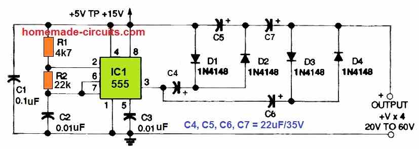
Voltage Tripler Circuit
The circuit for the DC voltage quadrupler is depicted in the following figure and may produce output voltages between 20 and 60 volts.

Negative Voltage Doubler Circuit
This diagram illustrates the next circuit configuration for a DC negative-voltage generator. It could generate an output voltage with a negative polarity and an amplitude that is approximately two times that of the earlier generator.

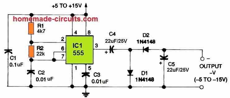
Moreover, it operates at 3 Hz and supplies power to an output stage that consists of the diodes D1 and D2 and the capacitors C4 and C5. ICs that require either negative or positive power via a single polarity source could be powered by this circuit's split output.